DS18B20 Digital Temperature Sensor Temperature Measurement Example
1. DS18B20 digital temperature sensor.
This article will use the writing method of the three-stage state machine (Moore type) to operate the temperature measurement FPGA on the DS18B20 in order to understand the DS18B20 and become familiar with the writing method of the three-stage state machine.
1.1. Overview
Temperature transducer refers to a sensor that can sense temperature and convert it into a usable output signal. It is the most commonly used type of various sensors. With the development of modern instruments, miniaturization, integration, and digitization are becoming an important direction in the development of sensors.
The digital temperature sensor DS18B20 launched by DALLAS Semiconductor Company of the United States adopts a single bus protocol. That is, the interface with the FPGA only occupies one I/O port, without any external components, and directly converts the ambient temperature into a digital signal. Serial output in the form of digital code greatly simplifies the interface design between the sensor and FPGA.
The pins are as shown below:
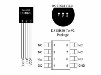 1.2. Structural composition
The measurement temperature range of DS18B20 is -55~+125℃, and the accuracy is ±0.5℃. The on-site (real-time) temperature is directly transmitted in a "single bus" digital manner, which greatly improves the system's anti-interference performance. It can directly read the measured temperature, and can realize 9~12-digit digital value reading mode through simple programming according to actual requirements. It works in the voltage range of 3~5.5V and adopts a variety of packaging forms, making the system design flexible and convenient. The set resolution and user-set alarm temperature are stored in EEPROM and will be retained after power off. Its internal structure is shown in the figure:
The structural block diagram of the cache is as follows:
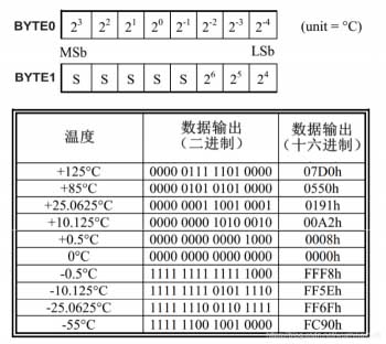
As can be seen from the above figure, the DS18B20 cache has a total of nine 8-bit registers, among which the low-order bit (LSB) of the temperature data corresponds to byte address 0, and the high-order bit (MSB) of the temperature data corresponds to byte address 1. By analogy, the byte address of the configuration register is 4. The format of temperature data storage is as follows:
 The DS18B20 is configured with 12-bit temperature data by default when it leaves the factory, of which the highest bit is the sign bit, that is, the temperature value has a total of 11 bits, and the lowest four bits are decimal places. When the FPGA reads temperature data, it reads 2 bytes at a time, totaling 16 bits. After reading, convert the lower 11-digit binary number into a decimal number and then multiply it by 0.0625 to get the actual measured temperature value.
In addition, it is necessary to judge the positive and negative temperature. The first 5 digits are sign bits. These 5 digits change at the same time, and we only need to judge any one of them. When the first five bits are 1, the read temperature is a negative value, and the measured value needs to be inverted, plus 1, and then multiplied by 0.0625 to get the actual temperature value. When the first five bits are 0, the temperature read is a positive value. Just multiply the measured value by 0.0625 to get the actual temperature value.
The fourth byte in the cache is the configuration register. The user can configure the resolution of DS18B20 by changing the values of R1 and R0. The power-on default is R1=1 and R0=1 (12-bit resolution). It should be noted that the conversion time is related to the resolution time. In addition, the highest bit and the lower 5 bits in the register are reserved for internal use and cannot be written. The relationship between conversion time and number of digits is shown in the following table:
1.3. Communication steps
How to operate DS18B20 to convert and read temperature? Proceed as follows:
1. Initialization
All events on the 1-Wire bus must begin with initialization. The initialization sequence consists of a reset pulse from the master on the bus followed by a presence pulse in response from the slave. This presence pulse lets the bus master know that the DS18B20 is on the bus and ready to operate. All specific timings are introduced in Chapter 1.4.
2. ROM command
When initialization is complete, ROM commands can be executed. These commands operate on the 64-bit ROM code of each device and can be used to identify each device when multiple devices are connected to the bus. There are a total of 5 ROM commands, each command is 8 bits in length.
Search ROM[F0h]: When the system is powered on and initialized, the master device can identify the ROM codes of all slave devices on the bus. This allows the master device to determine the type and number of slave devices on the bus.
Read ROM[33h]: This command allows the master device to read the 64-bit ROM code of the DS18B20. This command can only be used when there is only one DS18B20 on the bus. If there are multiple slave devices on the bus, sending this command will cause data conflicts when all slave devices will respond.
Match ROM[55h]: The Match ROM command is followed by a 64-bit ROM code that allows the master to locate a specific DS18B20 on the multidrop bus. Only DS18B20s that exactly match the 64-bit ROM sequence will respond. All other slave devices on the bus will wait for the next reset pulse. This command can be used when there are single or multiple devices on the bus.
Skip ROM[CCh]: This command can proceed to the next step without providing the 64-bit ROM code, which can save time in the case of a single-point bus (a DS18B20 sensor). If there is more than one slave device on the bus, and a read command is issued after skipping the ROM command, all slave devices will perform temperature conversions at the same time, and a data conflict will occur on the bus.
Alarm Search [ECh]: The operation of this command is basically the same as the Skip ROM command, but the difference is that only slave devices with a temperature above TH or below TL (reaching an alarm condition) will respond. As long as there is no power outage, the alarm status will remain until the temperature is no longer within the alarm range.
 3. Function commands
When the master device on the bus determines which DS18B20 can communicate through a ROM command, the master device can send a function command to one of the slave devices. These commands allow the master device to control the slave device to perform a series of operations.
Temperature conversion [44h]: This command initializes a single temperature conversion. After the temperature conversion is completed, the converted temperature data will be stored in byte0 (lower eight bits of temperature data) and byte1 (higher eight bits of temperature data) in the cache, and then the DS18B20 returns to the low-power idle state. If the bus issues a read time slot after this command, the DS18B20 will respond with a "0" if a temperature conversion is in progress, or a "1" if the temperature conversion is completed. If the "parasitic power supply" power supply mode is used, the bus should be forced to be pulled high immediately after the command is issued, and the pull-up time should be greater than the timing requirements.
Write scratchpad [4Eh]: This command causes the master device to write 3 bytes of data to the cache. The first byte is written to byte2 of the cache (TH register), the second byte of data is written to byte3 (TL register), and the third byte of data is written to byte4 (configuration register). All data is written sequentially from low bit to high bit. A reset can interrupt writing at any time.
Read the cache [BEh]: Read the value in the cache, starting from byte0 (the lower eight bits of temperature) and reading to byte8 (CRC check). Each byte of data is transmitted starting from the lower bit. If you don't want to read so much data, you can terminate it by resetting at any time when reading data.
Copy cache [48h]: This command copies the values in TH (byte2), TL (byte3) and configuration register (byte4) in the cache to the non-volatile memory EEPROM. If the bus controller issues a read time slot after this command and the DS18B20 is busy copying the scratchpad to the EEPROM memory, the DS18B20 will output a "0". If the copy is completed, the DS18B20 will output a "1". If the device is powered in "parasitic power" mode, the bus must be forced high for at least 10ms immediately after this command is sent.
Recall EEPROM[B8h]: This command recalls the temperature alarm trigger value (TH and TL) and configuration register data from EEPROM to the cache. This operation will be automatically performed once after power-on, so there will always be valid data in the temporary register during power-on. If the read time slot is initiated after the recall command, the DS18B20 will respond with "0" if the recall of the EEPROM is in progress and "1" if the recall is complete.
Read power supply mode [B4h]: This command can read whether the DS18B20 on the bus is powered by a "parasitic power supply". In the reading data timing sequence, "0" indicates "parasitic power supply" mode power supply, and "1" indicates external power supply.
This article will use the writing method of the three-stage state machine (Moore type) to operate the temperature measurement FPGA on the DS18B20 in order to understand the DS18B20 and become familiar with the writing method of the three-stage state machine.
 |
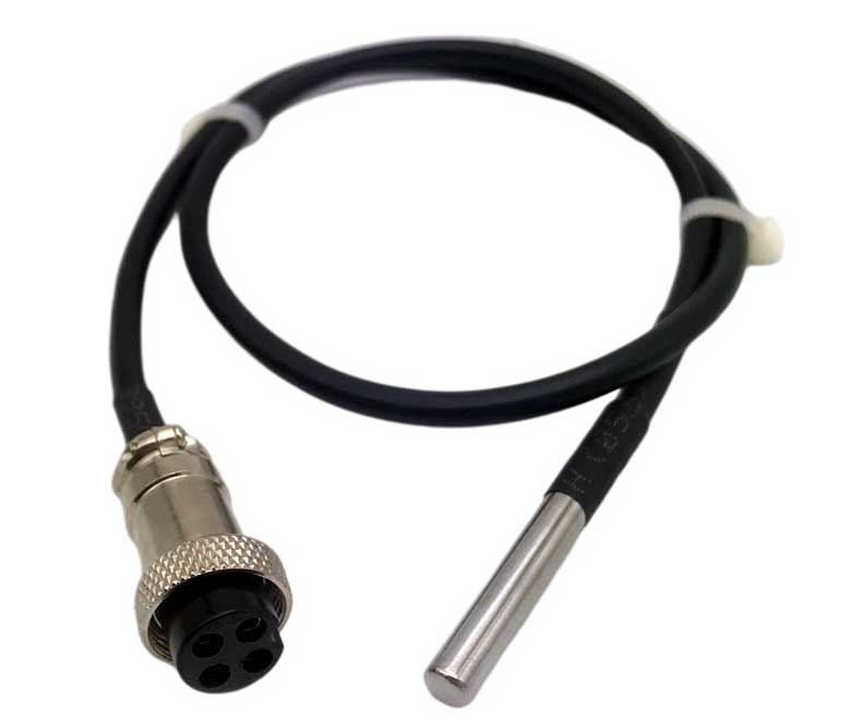 |
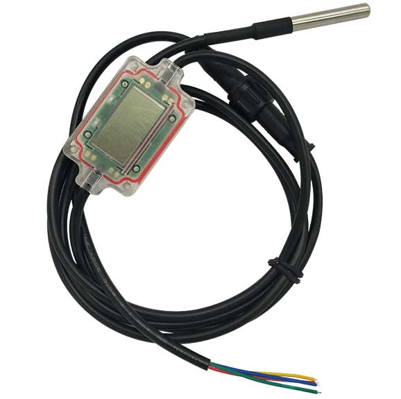
| ds18b20 to rs485 temperature and humidity sensor acquisition probe | ds18b20 sensor probe and connector |
1.1. Overview
Temperature transducer refers to a sensor that can sense temperature and convert it into a usable output signal. It is the most commonly used type of various sensors. With the development of modern instruments, miniaturization, integration, and digitization are becoming an important direction in the development of sensors.
The digital temperature sensor DS18B20 launched by DALLAS Semiconductor Company of the United States adopts a single bus protocol. That is, the interface with the FPGA only occupies one I/O port, without any external components, and directly converts the ambient temperature into a digital signal. Serial output in the form of digital code greatly simplifies the interface design between the sensor and FPGA.
The pins are as shown below:
The measurement temperature range of DS18B20 is -55~+125℃, and the accuracy is ±0.5℃. The on-site (real-time) temperature is directly transmitted in a "single bus" digital manner, which greatly improves the system's anti-interference performance. It can directly read the measured temperature, and can realize 9~12-digit digital value reading mode through simple programming according to actual requirements. It works in the voltage range of 3~5.5V and adopts a variety of packaging forms, making the system design flexible and convenient. The set resolution and user-set alarm temperature are stored in EEPROM and will be retained after power off. Its internal structure is shown in the figure:
The structural block diagram of the cache is as follows:
As can be seen from the above figure, the DS18B20 cache has a total of nine 8-bit registers, among which the low-order bit (LSB) of the temperature data corresponds to byte address 0, and the high-order bit (MSB) of the temperature data corresponds to byte address 1. By analogy, the byte address of the configuration register is 4. The format of temperature data storage is as follows:
In addition, it is necessary to judge the positive and negative temperature. The first 5 digits are sign bits. These 5 digits change at the same time, and we only need to judge any one of them. When the first five bits are 1, the read temperature is a negative value, and the measured value needs to be inverted, plus 1, and then multiplied by 0.0625 to get the actual temperature value. When the first five bits are 0, the temperature read is a positive value. Just multiply the measured value by 0.0625 to get the actual temperature value.
The fourth byte in the cache is the configuration register. The user can configure the resolution of DS18B20 by changing the values of R1 and R0. The power-on default is R1=1 and R0=1 (12-bit resolution). It should be noted that the conversion time is related to the resolution time. In addition, the highest bit and the lower 5 bits in the register are reserved for internal use and cannot be written. The relationship between conversion time and number of digits is shown in the following table:
1.3. Communication steps
How to operate DS18B20 to convert and read temperature? Proceed as follows:
1. Initialization
All events on the 1-Wire bus must begin with initialization. The initialization sequence consists of a reset pulse from the master on the bus followed by a presence pulse in response from the slave. This presence pulse lets the bus master know that the DS18B20 is on the bus and ready to operate. All specific timings are introduced in Chapter 1.4.
2. ROM command
When initialization is complete, ROM commands can be executed. These commands operate on the 64-bit ROM code of each device and can be used to identify each device when multiple devices are connected to the bus. There are a total of 5 ROM commands, each command is 8 bits in length.
Search ROM[F0h]: When the system is powered on and initialized, the master device can identify the ROM codes of all slave devices on the bus. This allows the master device to determine the type and number of slave devices on the bus.
Read ROM[33h]: This command allows the master device to read the 64-bit ROM code of the DS18B20. This command can only be used when there is only one DS18B20 on the bus. If there are multiple slave devices on the bus, sending this command will cause data conflicts when all slave devices will respond.
Match ROM[55h]: The Match ROM command is followed by a 64-bit ROM code that allows the master to locate a specific DS18B20 on the multidrop bus. Only DS18B20s that exactly match the 64-bit ROM sequence will respond. All other slave devices on the bus will wait for the next reset pulse. This command can be used when there are single or multiple devices on the bus.
Skip ROM[CCh]: This command can proceed to the next step without providing the 64-bit ROM code, which can save time in the case of a single-point bus (a DS18B20 sensor). If there is more than one slave device on the bus, and a read command is issued after skipping the ROM command, all slave devices will perform temperature conversions at the same time, and a data conflict will occur on the bus.
Alarm Search [ECh]: The operation of this command is basically the same as the Skip ROM command, but the difference is that only slave devices with a temperature above TH or below TL (reaching an alarm condition) will respond. As long as there is no power outage, the alarm status will remain until the temperature is no longer within the alarm range.
When the master device on the bus determines which DS18B20 can communicate through a ROM command, the master device can send a function command to one of the slave devices. These commands allow the master device to control the slave device to perform a series of operations.
Temperature conversion [44h]: This command initializes a single temperature conversion. After the temperature conversion is completed, the converted temperature data will be stored in byte0 (lower eight bits of temperature data) and byte1 (higher eight bits of temperature data) in the cache, and then the DS18B20 returns to the low-power idle state. If the bus issues a read time slot after this command, the DS18B20 will respond with a "0" if a temperature conversion is in progress, or a "1" if the temperature conversion is completed. If the "parasitic power supply" power supply mode is used, the bus should be forced to be pulled high immediately after the command is issued, and the pull-up time should be greater than the timing requirements.
Write scratchpad [4Eh]: This command causes the master device to write 3 bytes of data to the cache. The first byte is written to byte2 of the cache (TH register), the second byte of data is written to byte3 (TL register), and the third byte of data is written to byte4 (configuration register). All data is written sequentially from low bit to high bit. A reset can interrupt writing at any time.
Read the cache [BEh]: Read the value in the cache, starting from byte0 (the lower eight bits of temperature) and reading to byte8 (CRC check). Each byte of data is transmitted starting from the lower bit. If you don't want to read so much data, you can terminate it by resetting at any time when reading data.
Copy cache [48h]: This command copies the values in TH (byte2), TL (byte3) and configuration register (byte4) in the cache to the non-volatile memory EEPROM. If the bus controller issues a read time slot after this command and the DS18B20 is busy copying the scratchpad to the EEPROM memory, the DS18B20 will output a "0". If the copy is completed, the DS18B20 will output a "1". If the device is powered in "parasitic power" mode, the bus must be forced high for at least 10ms immediately after this command is sent.
Recall EEPROM[B8h]: This command recalls the temperature alarm trigger value (TH and TL) and configuration register data from EEPROM to the cache. This operation will be automatically performed once after power-on, so there will always be valid data in the temporary register during power-on. If the read time slot is initiated after the recall command, the DS18B20 will respond with "0" if the recall of the EEPROM is in progress and "1" if the recall is complete.
Read power supply mode [B4h]: This command can read whether the DS18B20 on the bus is powered by a "parasitic power supply". In the reading data timing sequence, "0" indicates "parasitic power supply" mode power supply, and "1" indicates external power supply.


