Coding Instructions for DS18B20 Chip Sensor
ROM read-only memory used to store DS18B20ID code. The first 8 bits are the single-line series code (the code of DS18B20 is 19H), the next 48 bits are the unique serial number of the chip, and the last 8 bits are the CRC code (redundancy check) of the above 56 bits. The data is set at the time of production and cannot be changed by the user. DS18B20 has a total of 64-bit ROM.
RAM data scratchpad, used for internal calculations and data access. Data is lost after power failure. DS18B20 has a total of 9 bytes of RAM, each byte is 8 bits. The 1st and 2nd bytes are the data value information after temperature conversion, and the 3rd and 4th bytes are the image of the user EEPROM (commonly used for temperature alarm value storage). Its value will be refreshed during power-on reset. The fifth byte is the image of the user's third EEPROM. The 6th, 7th, and 8th bytes are counting registers, which are designed to allow users to obtain higher temperature resolution. It is also a temporary storage unit for internal temperature conversion and calculation. The 9th byte is the CRC code of the first 8 bytes. EEPROM is a non-volatile memory used to store data that needs to be saved for a long time, upper and lower temperature alarm values and verification data.
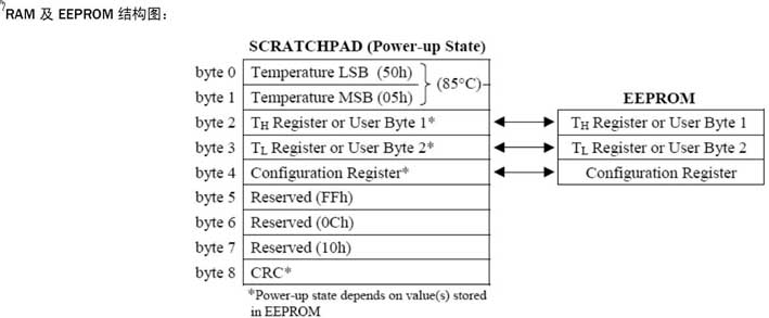
DS18B20 has a total of 3-bit EEPROM, and there are images in RAM to facilitate user operation.
Controller operation process for 18B20:
1. Reset: First we must reset the DS18B20 chip. Reset is a low-level signal of at least 480uS given by the controller (microcontroller) to the DS18B20 single bus. When 18B20 receives this reset signal, it will send back a chip presence pulse after 15~60uS.
2. Presence pulse: After the reset level ends, the controller should pull the data single bus high to receive the presence pulse after 15~60uS. The existence pulse is a low-level signal of 60~240uS. At this point, the communication parties have reached a basic agreement, and the next step will be data communication between the controller and 18B20. If the reset low level time is insufficient or the circuit of the single bus is broken, the presence pulse will not be received. Pay attention to handling unexpected situations when designing.
3. The controller sends a ROM command: After the two parties have finished greeting, the most important thing is to communicate. There are 5 ROM instructions in total, and only one can be sent in each working cycle. The ROM instructions are to read ROM data, specify matching chip, jump ROM, chip search, and alarm chip search. The ROM instruction is 8 bits in length and its function is to operate the on-chip 64-bit photolithography ROM. Its main purpose is to distinguish and process multiple devices connected to a bus. It is true that multiple devices can be connected to a single bus at the same time, and each device can be distinguished by its unique ID number. Generally, the ROM command can be skipped when only a single 18B20 chip is mounted (note: the skip ROM command here does not mean not sending a ROM command, but a unique "skip command")
4. The controller sends memory operation instructions: After the ROM instruction is sent to 18B20, the memory operation instruction is sent immediately (without interruption). The operation instructions are also 8 bits, 6 in total. The memory operation instructions are writing RAM data, reading RAM data, copying RAM data to EEPROM, temperature conversion, copying alarm values in EEPROM to RAM, and switching working modes. The function of the memory operation instruction is to command 18B20 to do what kind of work, which is the key to chip control.
5. Execution or data reading and writing: After a memory operation instruction is completed, the instruction execution or data reading and writing will be performed. This operation depends on the memory operation instruction. If the temperature conversion command is executed, the controller (microcontroller) must wait for 18B20 to execute its command. The general conversion time is 500uS. If you execute data read and write instructions, you need to strictly follow the 18B20 read and write timing. The methods of reading and writing data will be introduced in detail below.
To read out the current temperature data, we need to execute two working cycles. The first cycle is to reset, skip ROM instructions, execute temperature conversion memory operation instructions, and wait for 500uS temperature conversion time. Then the second cycle is executed to reset, skip ROM instructions, execute memory operation instructions to read RAM, and read data (up to 9 bytes, which can be stopped midway. To read only simple temperature values, read the first 2 bytes, that is, Can). Other operating procedures are similar and will not be introduced here.
DS28B20 chip ROM instruction list:
Read ROM [33H] (The hexadecimal command word in square brackets) This command allows the bus controller to read the 64-bit ROM of the DS18B20. This command can only be used when there is only one DS18B20 on the bus. If there is more than one hookup, data conflicts will occur when communicating.
Match ROM (specified matching chip) [55H]
This command is followed by a 64-bit serial number issued by the controller. When there are multiple DS18B20s on the bus, only the chip with the same serial number sent by the control can respond, and other chips will wait for the next reset. This command is suitable for single-chip and multi-chip mounting.
Skip ROM (skip ROM command) [CCH]
This instruction makes the chip not respond to ROM encoding. In the case of a single bus, this instruction can be selected to save time. If this command is used when mounting multiple chips, data conflicts will occur, resulting in errors.
Search ROM (search chip) [F0H]
After the chip is initialized, the search command allows a process of elimination to identify the 64-bit ROM of all devices when multiple chips are mounted on the bus.
Alarm Search (alarm chip search) [ECH]
In the case of multi-chip mounting, the alarm chip search command only responds to the chip whose temperature is higher than TH or lower than TL alarm condition. As long as the chip does not lose power, the alarm status will be maintained until the temperature is measured again and does not reach the alarm condition.
DS28B20 chip memory operation instruction list:
Write Scratchpad (write data to RAM) [4EH]
This is an instruction to write data to RAM. The two bytes of data written subsequently will be stored in address 2 (TH of alarm RAM) and address 3 (TL of alarm RAM). The reset signal can be used to abort writing during the writing process.
Read Scratchpad (read data from RAM) [BEH]
This instruction will read data from RAM. The read address starts from address 0 and can be read to address 9, completing the reading of the entire RAM data. The chip allows the reset signal to be used to abort reading during the reading process, that is, unnecessary subsequent bytes can not be read to reduce reading time.
Copy Scratchpad (Copy RAM data to EEPROM) [48H]
This instruction stores the data in RAM into EEPROM so that the data will not be lost when power is turned off. Since then, since the chip is busy with EEPROM storage processing, when the controller sends a read time gap, "0" is output on the bus. When the storage operation is completed, the bus will output "1". In parasitic working mode, a strong pull-up must be applied immediately after issuing this command and maintained for at least 10MS to maintain the chip operation.
Convert T (temperature conversion) [44H]
After receiving this command, the chip will perform a temperature conversion and put the converted temperature value into the 1st and 2nd addresses of the RAM. Since then, because the chip is busy with temperature conversion processing, when the controller sends a read time gap, "0" is output on the bus. When the storage operation is completed, the bus will output "1". In parasitic working mode, a strong pull-up must be applied immediately after issuing this command and maintained for at least 500MS to maintain the chip operation.
Recall EEPROM (copy the alarm value in EEPROM to RAM) [B8H]
This instruction copies the alarm value in EEPROM to the 3rd and 4th bytes in RAM. Since the chip is busy with copy processing, when the controller issues a read time slot, a "0" is output on the bus, and when the store operation is completed, a "1" is output on the bus. In addition, this command will be automatically executed when the chip is powered on and reset. In this way, the two alarm byte bits in RAM will always be a mirror image of the data in EEPROM.
Read Power Supply (working mode switching) [B4H]
After this command is issued and a read time gap is issued, the chip will return its power status word, "0" is the parasitic power status, and "1" is the external power status.
RAM data scratchpad, used for internal calculations and data access. Data is lost after power failure. DS18B20 has a total of 9 bytes of RAM, each byte is 8 bits. The 1st and 2nd bytes are the data value information after temperature conversion, and the 3rd and 4th bytes are the image of the user EEPROM (commonly used for temperature alarm value storage). Its value will be refreshed during power-on reset. The fifth byte is the image of the user's third EEPROM. The 6th, 7th, and 8th bytes are counting registers, which are designed to allow users to obtain higher temperature resolution. It is also a temporary storage unit for internal temperature conversion and calculation. The 9th byte is the CRC code of the first 8 bytes. EEPROM is a non-volatile memory used to store data that needs to be saved for a long time, upper and lower temperature alarm values and verification data.
DS18B20 has a total of 3-bit EEPROM, and there are images in RAM to facilitate user operation.
Controller operation process for 18B20:
1. Reset: First we must reset the DS18B20 chip. Reset is a low-level signal of at least 480uS given by the controller (microcontroller) to the DS18B20 single bus. When 18B20 receives this reset signal, it will send back a chip presence pulse after 15~60uS.
2. Presence pulse: After the reset level ends, the controller should pull the data single bus high to receive the presence pulse after 15~60uS. The existence pulse is a low-level signal of 60~240uS. At this point, the communication parties have reached a basic agreement, and the next step will be data communication between the controller and 18B20. If the reset low level time is insufficient or the circuit of the single bus is broken, the presence pulse will not be received. Pay attention to handling unexpected situations when designing.
3. The controller sends a ROM command: After the two parties have finished greeting, the most important thing is to communicate. There are 5 ROM instructions in total, and only one can be sent in each working cycle. The ROM instructions are to read ROM data, specify matching chip, jump ROM, chip search, and alarm chip search. The ROM instruction is 8 bits in length and its function is to operate the on-chip 64-bit photolithography ROM. Its main purpose is to distinguish and process multiple devices connected to a bus. It is true that multiple devices can be connected to a single bus at the same time, and each device can be distinguished by its unique ID number. Generally, the ROM command can be skipped when only a single 18B20 chip is mounted (note: the skip ROM command here does not mean not sending a ROM command, but a unique "skip command")
4. The controller sends memory operation instructions: After the ROM instruction is sent to 18B20, the memory operation instruction is sent immediately (without interruption). The operation instructions are also 8 bits, 6 in total. The memory operation instructions are writing RAM data, reading RAM data, copying RAM data to EEPROM, temperature conversion, copying alarm values in EEPROM to RAM, and switching working modes. The function of the memory operation instruction is to command 18B20 to do what kind of work, which is the key to chip control.
5. Execution or data reading and writing: After a memory operation instruction is completed, the instruction execution or data reading and writing will be performed. This operation depends on the memory operation instruction. If the temperature conversion command is executed, the controller (microcontroller) must wait for 18B20 to execute its command. The general conversion time is 500uS. If you execute data read and write instructions, you need to strictly follow the 18B20 read and write timing. The methods of reading and writing data will be introduced in detail below.
To read out the current temperature data, we need to execute two working cycles. The first cycle is to reset, skip ROM instructions, execute temperature conversion memory operation instructions, and wait for 500uS temperature conversion time. Then the second cycle is executed to reset, skip ROM instructions, execute memory operation instructions to read RAM, and read data (up to 9 bytes, which can be stopped midway. To read only simple temperature values, read the first 2 bytes, that is, Can). Other operating procedures are similar and will not be introduced here.
 |
 |
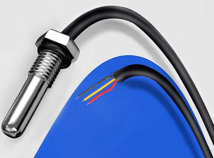
| Magnetic DS18B20 digital sensor | Control instructions of DS18B20 digital sensor |
DS28B20 chip ROM instruction list:
Read ROM [33H] (The hexadecimal command word in square brackets) This command allows the bus controller to read the 64-bit ROM of the DS18B20. This command can only be used when there is only one DS18B20 on the bus. If there is more than one hookup, data conflicts will occur when communicating.
Match ROM (specified matching chip) [55H]
This command is followed by a 64-bit serial number issued by the controller. When there are multiple DS18B20s on the bus, only the chip with the same serial number sent by the control can respond, and other chips will wait for the next reset. This command is suitable for single-chip and multi-chip mounting.
Skip ROM (skip ROM command) [CCH]
This instruction makes the chip not respond to ROM encoding. In the case of a single bus, this instruction can be selected to save time. If this command is used when mounting multiple chips, data conflicts will occur, resulting in errors.
Search ROM (search chip) [F0H]
After the chip is initialized, the search command allows a process of elimination to identify the 64-bit ROM of all devices when multiple chips are mounted on the bus.
Alarm Search (alarm chip search) [ECH]
In the case of multi-chip mounting, the alarm chip search command only responds to the chip whose temperature is higher than TH or lower than TL alarm condition. As long as the chip does not lose power, the alarm status will be maintained until the temperature is measured again and does not reach the alarm condition.
DS28B20 chip memory operation instruction list:
Write Scratchpad (write data to RAM) [4EH]
This is an instruction to write data to RAM. The two bytes of data written subsequently will be stored in address 2 (TH of alarm RAM) and address 3 (TL of alarm RAM). The reset signal can be used to abort writing during the writing process.
Read Scratchpad (read data from RAM) [BEH]
This instruction will read data from RAM. The read address starts from address 0 and can be read to address 9, completing the reading of the entire RAM data. The chip allows the reset signal to be used to abort reading during the reading process, that is, unnecessary subsequent bytes can not be read to reduce reading time.
Copy Scratchpad (Copy RAM data to EEPROM) [48H]
This instruction stores the data in RAM into EEPROM so that the data will not be lost when power is turned off. Since then, since the chip is busy with EEPROM storage processing, when the controller sends a read time gap, "0" is output on the bus. When the storage operation is completed, the bus will output "1". In parasitic working mode, a strong pull-up must be applied immediately after issuing this command and maintained for at least 10MS to maintain the chip operation.
Convert T (temperature conversion) [44H]
After receiving this command, the chip will perform a temperature conversion and put the converted temperature value into the 1st and 2nd addresses of the RAM. Since then, because the chip is busy with temperature conversion processing, when the controller sends a read time gap, "0" is output on the bus. When the storage operation is completed, the bus will output "1". In parasitic working mode, a strong pull-up must be applied immediately after issuing this command and maintained for at least 500MS to maintain the chip operation.
Recall EEPROM (copy the alarm value in EEPROM to RAM) [B8H]
This instruction copies the alarm value in EEPROM to the 3rd and 4th bytes in RAM. Since the chip is busy with copy processing, when the controller issues a read time slot, a "0" is output on the bus, and when the store operation is completed, a "1" is output on the bus. In addition, this command will be automatically executed when the chip is powered on and reset. In this way, the two alarm byte bits in RAM will always be a mirror image of the data in EEPROM.
Read Power Supply (working mode switching) [B4H]
After this command is issued and a read time gap is issued, the chip will return its power status word, "0" is the parasitic power status, and "1" is the external power status.


