Summary of simple overcurrent protection circuit design
Working Principle of Overcurrent Protection Circuit
When the circuit is in normal state, the current of PTC thermistor for over-current protection is less than the rated current, and the PTC thermistor for over-current protection is in normal state, and the resistance value is very small, which will not affect the normal operation of the protected circuit. When the circuit fails and the current greatly exceeds the rated current, the PTC thermistor for overcurrent protection suddenly heats up and is in a high-impedance state, so that the circuit is in a relatively "To break off" state, thereby protecting the circuit from damage. When the fault is removed, the PTC thermistor for overcurrent protection also automatically returns to the low resistance state, and the circuit resumes normal operation.
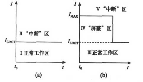
When the load current exceeds the limit current ILIMIT is not too much and the duration is not too long, we hope that the over-current protection circuit can keep the LDO working uninterruptedly. Therefore, it is necessary to use "shielding" mode to shield the over-current signal which can keep LDO running uninterruptedly. For over-current signal whose amplitude and duration exceed the range, the over-current protection circuit can adopt the mode of interrupting LDO operation. The traditional "interrupt" mode current protection circuit operating state is shown in Figure 1 (a), divided into normal working area I and "interrupt" area II. When the load current does not exceed ILIMIT, the LDO operates in the normal operating region and the LDO enters the "interrupt" region when the load current exceeds ILIMIT. The working state of the overcurrent protection circuit after adding the "shield" mode is as shown in Fig. 1(b), which is divided into normal working area III, shielding area IV and interruption area V. When the load current is less than ILIMIT, the LDO is in the normal working area. When the amplitude of the overcurrent signal is between ILIMIT and the maximum amplitude current IMAX, and the duration of the action is within t=tMAX, that is, ILIMIT≤ILOAD≤IMAX, t≤tMAX, the LDO enters the shielding area, outside the range. The overcurrent signal will enter the interrupt zone. Comparing Figures 1(a) and (b), it can be seen that the normal working area of the LDO after the overcurrent protection circuit is improved includes the normal working area III and the "shielding" area IV of Fig. 1(b). Increase the scope of the work area and improve the working efficiency of the LDO.
The overall block diagram of the LDO including the overcurrent protection circuit is shown in Figure 2. To the left of the dashed line is the LDO body circuit, which includes the error amplifier, power tube, load resistor, and voltage divider resistor. The right part of the dotted line is the current protection circuit. The main function is to sense and detect whether the load current exceeds the limit current, and then control the power tube to determine whether to interrupt the operation of the LDO, including the current sensing circuit and the control circuit. The traditional overcurrent protection circuit only adopts the "interrupt" mode (excluding the virtual frame) shown in the real frame II in Fig. 2. For any load overcurrent condition, the LDO is interrupted regardless of the duration of the action; Based on the traditional "interrupt" mode, this paper adds "shield" mode (virtual box I in Figure 2), which can effectively shield the over-current signal that LDO wants to work uninterruptedly, and make LDO run more efficiently while retaining the "interrupt" mode. Ensure that LDOs work safely.
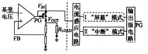
figure 2 LDO block diagram with overcurrent protection circuit
shield" mode circuit implementation
Figure 3 is a circuit diagram of the overcurrent protection before and after the improvement. The unframed portion is a conventional "interrupt" mode overcurrent protection circuit consisting of a current sensing circuit, a comparison circuit, and an output stage circuit. The current sensing circuit samples the power tube current. The sampled current and the limiting current ILIMIT are converted into two comparator voltages VSENSE and VLIMIT, respectively, and compared to obtain a VCO. The VCO acts on the output stage circuit to control the power tube gate voltage. If the load is overcurrent, the overcurrent protection circuit causes the power transistor gate voltage PG to be high, forcing the LDO interrupt.
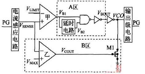
image 3 Improved current protection circuit diagram
The circuit of the B-zone of the virtual frame in Fig. 3 can solve the problem that the large current in the shielding time may cause the power tube to burn instantaneously. When a large overcurrent signal occurs during the delay time, the power tube can be turned off in time to ensure system safety. The shutdown circuit consists of a comparator B and an NMOS switch M1.
When the overcurrent signal exceeds the maximum limit current IMAX (VSENSE VMAX at this time), the VCOUT output of comparator B is high, which leads to the switch M1 turn-on, so that the strong behavior of VCO is low without the influence of the shielding circuit and the LDO is synchronously turned off to ensure the safety of the power transistor. When the overcurrent is not too large, the comparator output voltage VCOUT is low, and the switch M1 is not turned on, which does not affect the operation of the shield circuit.
The improved current protection circuit shown in Figure 3 is capable of achieving the desired "shield" zone mode of operation as illustrated in Figure 1(b). The load current overcurrent maximum sustained action time tMAX and the maximum overcurrent amplitude IMAX are the time and amplitude boundaries of the "shield" region. In practical applications, the thermal power and breakdown current that the power tube can withstand is limited. The maximum duration of action tMAX is determined by the thermal power dissipation and thermal performance that the power tube can withstand, while the maximum breakdown current of the power tube determines the maximum amplitude IMAX of the overcurrent.
For specific application needs, the LDO can be operated more efficiently by setting a reasonable masking time and maximum overcurrent amplitude.
The logic relationship of the "shield" mode is shown in Figure 4, where VB1 and VCOUT are the output signals of comparators A and B, respectively. After a delay time, VB1 outputs VB2, the output voltage of the shield circuit is VBOUT, and the VCO is the output of the shield circuit. The waveforms of VB1, VB2, and VBOUT reflect the logic relationship of the shield circuit. VBOUT is low only when VB1 and VB2 are high at the same time, otherwise VBOUT is always high. Therefore, the shielding circuit shields the pulse signal within the delay time and maintains the wide pulse signal; VCOUT is the enable, as long as VCOUT is high, the VCO goes low immediately.
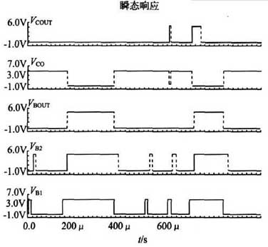
Figure 4 "shield" circuit logic diagram
When the circuit is in normal state, the current of PTC thermistor for over-current protection is less than the rated current, and the PTC thermistor for over-current protection is in normal state, and the resistance value is very small, which will not affect the normal operation of the protected circuit. When the circuit fails and the current greatly exceeds the rated current, the PTC thermistor for overcurrent protection suddenly heats up and is in a high-impedance state, so that the circuit is in a relatively "To break off" state, thereby protecting the circuit from damage. When the fault is removed, the PTC thermistor for overcurrent protection also automatically returns to the low resistance state, and the circuit resumes normal operation.
Simple overcurrent protection circuit design
Traditional over-current protection circuit consists of current induction circuit, comparison circuit and output stage, which is divided into constant-current over-current protection and return over-current protection. The traditional overcurrent protection circuit uses an "interrupt" mode. For any overcurrent condition, as long as the load current is greater than the limiting current, the LDO will be interrupted.When the load current exceeds the limit current ILIMIT is not too much and the duration is not too long, we hope that the over-current protection circuit can keep the LDO working uninterruptedly. Therefore, it is necessary to use "shielding" mode to shield the over-current signal which can keep LDO running uninterruptedly. For over-current signal whose amplitude and duration exceed the range, the over-current protection circuit can adopt the mode of interrupting LDO operation. The traditional "interrupt" mode current protection circuit operating state is shown in Figure 1 (a), divided into normal working area I and "interrupt" area II. When the load current does not exceed ILIMIT, the LDO operates in the normal operating region and the LDO enters the "interrupt" region when the load current exceeds ILIMIT. The working state of the overcurrent protection circuit after adding the "shield" mode is as shown in Fig. 1(b), which is divided into normal working area III, shielding area IV and interruption area V. When the load current is less than ILIMIT, the LDO is in the normal working area. When the amplitude of the overcurrent signal is between ILIMIT and the maximum amplitude current IMAX, and the duration of the action is within t=tMAX, that is, ILIMIT≤ILOAD≤IMAX, t≤tMAX, the LDO enters the shielding area, outside the range. The overcurrent signal will enter the interrupt zone. Comparing Figures 1(a) and (b), it can be seen that the normal working area of the LDO after the overcurrent protection circuit is improved includes the normal working area III and the "shielding" area IV of Fig. 1(b). Increase the scope of the work area and improve the working efficiency of the LDO.
The overall block diagram of the LDO including the overcurrent protection circuit is shown in Figure 2. To the left of the dashed line is the LDO body circuit, which includes the error amplifier, power tube, load resistor, and voltage divider resistor. The right part of the dotted line is the current protection circuit. The main function is to sense and detect whether the load current exceeds the limit current, and then control the power tube to determine whether to interrupt the operation of the LDO, including the current sensing circuit and the control circuit. The traditional overcurrent protection circuit only adopts the "interrupt" mode (excluding the virtual frame) shown in the real frame II in Fig. 2. For any load overcurrent condition, the LDO is interrupted regardless of the duration of the action; Based on the traditional "interrupt" mode, this paper adds "shield" mode (virtual box I in Figure 2), which can effectively shield the over-current signal that LDO wants to work uninterruptedly, and make LDO run more efficiently while retaining the "interrupt" mode. Ensure that LDOs work safely.
figure 2 LDO block diagram with overcurrent protection circuit
shield" mode circuit implementation
Figure 3 is a circuit diagram of the overcurrent protection before and after the improvement. The unframed portion is a conventional "interrupt" mode overcurrent protection circuit consisting of a current sensing circuit, a comparison circuit, and an output stage circuit. The current sensing circuit samples the power tube current. The sampled current and the limiting current ILIMIT are converted into two comparator voltages VSENSE and VLIMIT, respectively, and compared to obtain a VCO. The VCO acts on the output stage circuit to control the power tube gate voltage. If the load is overcurrent, the overcurrent protection circuit causes the power transistor gate voltage PG to be high, forcing the LDO interrupt.
image 3 Improved current protection circuit diagram
If we add the circuit structure shown in the A area of the virtual box in Figure 3, the circuit will become "shielded" mode current protection. The shielding circuit is composed of a delay circuit or a NOT gate. The signal VB1 outputted by the comparator A is delayed to obtain VB2, and VB1 and VB2 are subjected to NAND operation and then reversed to obtain the output signal VBOUT of the mask circuit.
Since the logical OR operation can only keep the two signals at the same time unchanged, the pulse signal within the delay time can be eliminated by the NOR gate and the inverter. Adding a shield circuit to the overcurrent protection circuit shields the overcurrent signal during the delay time. However, if the load current is too large, the power tube may be burned in an instant, so a corresponding shutdown circuit is required. When the load current exceeds the maximum limit current IMAX, the overcurrent protection circuit can directly turn off the LDO without delay.
Since the logical OR operation can only keep the two signals at the same time unchanged, the pulse signal within the delay time can be eliminated by the NOR gate and the inverter. Adding a shield circuit to the overcurrent protection circuit shields the overcurrent signal during the delay time. However, if the load current is too large, the power tube may be burned in an instant, so a corresponding shutdown circuit is required. When the load current exceeds the maximum limit current IMAX, the overcurrent protection circuit can directly turn off the LDO without delay.
The circuit of the B-zone of the virtual frame in Fig. 3 can solve the problem that the large current in the shielding time may cause the power tube to burn instantaneously. When a large overcurrent signal occurs during the delay time, the power tube can be turned off in time to ensure system safety. The shutdown circuit consists of a comparator B and an NMOS switch M1.
When the overcurrent signal exceeds the maximum limit current IMAX (VSENSE VMAX at this time), the VCOUT output of comparator B is high, which leads to the switch M1 turn-on, so that the strong behavior of VCO is low without the influence of the shielding circuit and the LDO is synchronously turned off to ensure the safety of the power transistor. When the overcurrent is not too large, the comparator output voltage VCOUT is low, and the switch M1 is not turned on, which does not affect the operation of the shield circuit.
The improved current protection circuit shown in Figure 3 is capable of achieving the desired "shield" zone mode of operation as illustrated in Figure 1(b). The load current overcurrent maximum sustained action time tMAX and the maximum overcurrent amplitude IMAX are the time and amplitude boundaries of the "shield" region. In practical applications, the thermal power and breakdown current that the power tube can withstand is limited. The maximum duration of action tMAX is determined by the thermal power dissipation and thermal performance that the power tube can withstand, while the maximum breakdown current of the power tube determines the maximum amplitude IMAX of the overcurrent.
For specific application needs, the LDO can be operated more efficiently by setting a reasonable masking time and maximum overcurrent amplitude.
The logic relationship of the "shield" mode is shown in Figure 4, where VB1 and VCOUT are the output signals of comparators A and B, respectively. After a delay time, VB1 outputs VB2, the output voltage of the shield circuit is VBOUT, and the VCO is the output of the shield circuit. The waveforms of VB1, VB2, and VBOUT reflect the logic relationship of the shield circuit. VBOUT is low only when VB1 and VB2 are high at the same time, otherwise VBOUT is always high. Therefore, the shielding circuit shields the pulse signal within the delay time and maintains the wide pulse signal; VCOUT is the enable, as long as VCOUT is high, the VCO goes low immediately.
Figure 4 "shield" circuit logic diagram


